We All Provide TEG & Solutions for JISSO.
KITPRODUCTS
KIT製品一覧表
| Product | Ni/Au |
Cu |
Cu +OSP |
E-679FG SAC |
E-700G SAC |
E-705G SAC |
E-700G NiPdAu+ SAC |
E-705G NiPdAu+ SAC |
NiPdAu |
|---|---|---|---|---|---|---|---|---|---|
| CC80 | - | ● | ● | - | - | - | - | - | - |
| FC150LC-1×1 | - | - | - | - | - | - | - | ● | - |
| FC120-1×1 | - | ● | ● | - | - | ● | - | - | - |
| FC120-2×2 | - | ● | ● | - | - | ● | - | - | - |
| FC150-1×1 | ● | ● | ● | ● | - | - | - | - | - |
| FC150-2×2 | - | ● | ● | - | ● | - | - | - | - |
| FC200-1×1 | ● | ● | ● | ● | - | - | - | - | - |
| FC200-2×2 | ● | - | - | - | ● | - | - | - | - |
| WLP300P/400P | ● | - | - | - | - | - | - | - | - |
その他のKIT製品
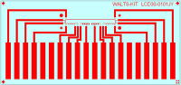
- WALTS-TEG IP40-0101JY *Silicon Interposer
- WALTS-TEG IP40A-0101JY *Silicon Interposer
- WALTS-TEG IP80-0101JY *Silicon Interposer
- WALTS-KIT LCD30-0101JY
- WALTS-KIT COF30-0101JY
KIT製品詳細
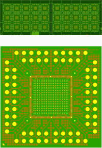
WALTS-KIT CC80(T)-0106JY【MAP】
| Specification | WALTS-KIT CC80(T)-0106JY【MAP】 |
|---|---|
| Structure | 1-2-1 Build up Substrate |
| Layer Structure | Layer 1, 2 Signal Layer(Via) Layer 3, 4 Mesh |
| Outline | 187.5mm×64.0mm×t(0.36mm) |
| Material | Core: HL832NSF Build Layer: GHPL-830NSF |
| Solder Resist Material | PSR4000 AUS-308 |
| Lead Min L/S | 32µm/48µm |
| Number of Lead | 648 |
| Pad Dimensions | φ0.75mm (SR opening: φ0.67mm) |
| Number of Measurement Pad | 72 pads |
| Electrode |
Cu + OSP |
WALTS-KIT CC80CL-0100JY【MAP】
| Specification | WALTS-KIT CC80CL-0100JY【MAP】 |
|---|---|
| Structure | Coreless 3L |
| Layer Structure | Layer 1, 2 Signal Layer(Via) Layer 3 Mesh |
| Outline | 187.5mm×64.0mm×t(0.16mm) |
| Material | Build Layer: GHPL-830NSF |
| Solder Resist Material | PSR4000 AUS-308 |
| Lead Min L/S | 32µm/48µm |
| Number of Lead | 648 |
| Pad Dimensions | φ0.75mm (SR opening: φ0.67mm) |
| Number of Measurement Pad | 72 pads |
| Electrode |
Cu Cu + OSP |
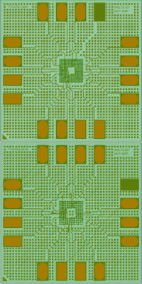
WALTS-KIT FC150LC(S)-0303JY
| Specification | WALTS-KIT FC150LC(S)-0303JY |
|---|---|
| Layer Structure | 2-2-2 Build up Substrate |
| Outline | 55.0mm×55.0mm×t(0.66mm) |
| Material | Build Layer:ABF-GX13 |
| Solder Resist | PSR4000 AUS-703 |
| Land Size | φ0.13mm● |
| Number of Lead | 25921 (161×161) |
| SR Opening | φ85μm● |
| Number of Measurement Pad | 240 pads |
| Daisy Pattern | ① Daisy Chain Pattern A: 196 Pads(14×14) ② Daisy Chain Pattern B: 72 Pads(12×6) ③ Daisy Chain Pattern C: 169 Pads(13×13) ④ Daisy Pattern D: 12 Pads(4×3) |
| Electrode | Electroless Plating: Ni/Pd/Au Electroless Plating: Ni/Pd/Au+SnAgCu |
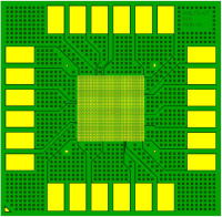
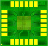
WALTS-KIT 01A120P(S)-10 1×1
-10.jpg)
| Specification | WALTS-01A120P(S)-10 1×1 |
|---|---|
| Structure | Rigid Substrate (Both) |
| Outline | 30.0mm×30.0mm×t(0.97mm) |
| Material | Core: MCL-E-705G Build Layer:ABF-GX92 |
| Solder Resist | PSR4000 AUS-703 |
| Land Size | φ0.095mm● |
| Number of Lead | 5776 (76×76) |
| SR Opening | φ70μm● |
| Number of Measurement Pad | 24 pads |
| Daisy Chain | Center Area 18×20 Matrix Corner Area 19×20 four Matrix |
| Electrode | Cu + OSP (option Solder Coat) *OSP: Organic Solderability Preservatives |
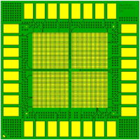
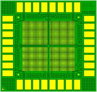
WALTS-KIT FC120(S)-101JY 2×2
.jpg)
| Specification | WALTS-FC120(S)-0101JY 2×2 |
|---|---|
| Structure | Rigid Substrate (Both) |
| Outline | 35.0mm×35.0mm×t(0.97mm) |
| Material | Core: MCL-E-705G Build Layer:ABF-GX92 |
| Solder Resist | PSR4000 AUS-703 |
| Land Size | φ0.095mm● |
| Number of Lead | 23104 (5776/chip×4) |
| SR Opening | φ70μm● |
| Number of Measurement Pad | 32 pads |
| Daisy Chain | Center Area 38×40 Matrix Corner Area 19×20 four Matrix |
| Electrode | Cu + OSP (option Solder Coat) *OSP: Organic Solderability Preservatives |
WALTS-KIT 01A150P(S)-10-3 1×1
| Specification | WALTS-KIT 01A150P(S)-10-3 1×1 |
|---|---|
| Structure | Rigid Substrate (Both) |
| Outline | 30.0mm×30.0mm×t(0.98mm) |
| Material | Build Layer:ABF-GX92 |
| Solder Resist | PSR4000 AUS-703 |
| Land Size | φ0.12mm● |
| Number of Lead | 3721 (61×61) |
| SR Opening | φ80μm● |
| Number of Measurement Pad | 24 pads |
| Daisy Chain | Center Area 16×15 Matrix Corner Area 15×15 four Matrix |
| Electrode | Cu + OSP (option Solder Coat) Electroless Ni/Au Plating *OSP: Organic Solderability Preservatives |
WALTS-KIT FC150(S)-0106JY 2×2(E-700G)
| Specification | WALTS-KIT FC150(S)-0106JY 2×2 (E-700G) |
|---|---|
| Structure | Rigid Substrate (Both) |
| Outline | 35.0mm×35.0mm×t(0.98mm) |
| Material | Build Layer:ABF-GX92 |
| Solder Resist | PSR4000 AUS-703 |
| Land Size | φ0.12mm● |
| Number of Lead | 14884 (3721/chip×4) |
| SR Opening | φ80μm● |
| Number of Measurement Pad | 32 pads |
| Daisy Chain | Center Area 30×30 Matrix Corner Area 15×15 four Matrix |
| Electrode | Cu + OSP (option Solder Coat) *OSP: Organic Solderability Preservatives |
WALTS-KIT 01A200P(S)-10-2 1×1
| Specification | WALTS-KIT 01A200P(S)-10-2 1×1 |
|---|---|
| Structure | Rigid Substrate (Both) |
| Outline | 30.0mm×30.0mm×t(0.97mm) |
| Core Material | Build Layer:ABF-GX92 |
| Solder Resist | PSR4000 AUS-703 |
| Land Size | φ0.14mm● |
| Number of Lead | 2116 (46×46) |
| Vehicle | 10mm×10mm 200μm pitch area |
| SR Opening | φ95μm● |
| Number of Measurement Pad | 24 pads |
| Daisy Chain | Center Area 12×12 Matrix Corner Area 12×11 four Matrix |
| Electrode | Cu + OSP (option Solder Coat) *OSP: Organic Solderability Preservatives |
WALTS-KIT FC200-0102JY 2×2
| Specification | WALTS-KIT FC200-0102JY 2×2 |
|---|---|
| Structure | Rigid Substrate (Both) |
| Outline | 35.0mm×35.0mm×t(0.87mm) |
| Material |
core: E-700GR |
| Solder Resist | PSR4000 AUS-703 |
| Land Size | φ0.14mm● |
| Number of Lead | 8464 (2116/chip×4) |
| Vehicle | 20mm×20mm 200μm pitch area |
| SR Opening | φ95μm● |
| Number of Measurement Pad | 32 pads |
| Daisy Chain | Center Area 20×18 Matrix Corner Area 12×11 four Matrix |
| Electrode | Cu + OSP (option Solder Coat) *OSP: Organic Solderability Preservatives |
WALTS-KIT WLP(S)300P/400P-2
| Specification | WALTS-KIT WLP(S)300P/400P-2 * for WLP TEG (0.4mm pitch & 0.3mm pitch) |
|---|---|
| Structure | 1-2-1 Build up Substrate |
| Layer Structure | Layer1:WLP300P Layer4:WLP400P |
| Outline | 30.0mm×30.0mm×t(0.98mm) |
| Core Material | Core: E-679FGR Build Layer: ABF-GX13 |
| Solder Resist Material | PSR4000 AUS-703 |
| Number of Lead | WLP300P: 264 WLP400P: 144 |
| Pad Dimensions | 2.4mm×4.0mm (SR opening: 2.2mm×3.8mm) |
| Number of Measurement Pad | 15 pads |
| Electrode | Electroless Ni/Au plating |
WALTS-KIT LCD30A-0101JY
| Specification | WALTS-KIT LCD30A-0101JY |
|---|---|
| Material | Non Alkali Glass |
| Outline | 52.55mm×24.00mm×t(0.70mm) |
| Wire Material | ITO 1,500Å (option IZO) |
| Function | ‐‐Daisy Chain ‐‐Breakdown Voltage Check between the Bumps |
| Conformed Chip | WALTS-TEG LCD30A-0101JY |
WALTS-KIT COF30-0101JY
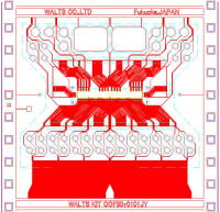
| Specification | WALTS-KIT COF30-0101JY |
|---|---|
| State | Reel |
| Product Name | S'PERFLEX |
| Plating Material | Sn |
| Conformed Chip | WALTS-TEG LCD30A-0101JY |
バナースペース
株式会社ウォルツ
〒819-1122
福岡県糸島市東1963-4
福岡超集積半導体ソリューション
センター303
TEL 092-332-1271
FAX 092-332-1281