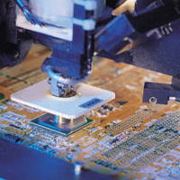

We open up next-generation assembly technology for semiconductor with leading-edge
technologies and information that we have developed over many years.As
the de facto standard, our products are used in the research and development
site world wide.Our well experienced architects can also custom-make TEG
to better suit your needs.A wide variety of film sputtering and deposition,
back grinding, dicing, bump forming, assembing and analysis are available.Our
high-quality service are all Made in Japan!
* TEG = Test Element Group * KIT = Test Kit
NEWS
V
- March.14.2025
- New catalog"Ver.30"released.
Click here「Contact Us」to receive our new catalog.
- Jun.1.2023
- New catalog"Ver.29"released.
- Dec.12.2022
- New catalog"Ver.28"released.
- Jan.31.2022
- New catalog"Ver.27"released.
- Dec.24.2019
- WALTS website updated!
WALTS-TEG WM40-0103JY
WALTS-TEG IPWM40-0101JY
WALTS-TEG HBM-T-0100JY
WALTS-TEG IPHBM-0100JY
WALTS-TEG FC120JY
WALTS-TEG FBW40A-0001JY
WLP-TEG (Free Size Cut)
WALTS-TEG HPW-MarkⅡ-0101JY
WALTS-TEG LCD30A-0101JY
WALTS-KIT 01A120P(S)-10
WALTS-KIT FC120(S)
SIPOS-TEG SI06
- July.2018
- New catalog"Ver.24"released.
- Sep.2015
- WALTS introduces new products!
<TEG>
WALTS-TEG MB130A-0101JY
WALTS-TEG CC40-0101JY
WALTS-TEG IP40-0101JY
WALTS-TEG IP40A-0101JY
WALTS-TEG CC80MarkⅡWM-0101JY
WALTS-TEG WM40-0101JY
WALTS-TEG WM40-0102JY
WALTS-TEG CC80MarkⅣ-0101JY(A/B)
WALTS-TEG IP80MarkⅣ-0101JY
WALTS-TEG FBW80-0001JY
WALTS-TEG STACTEG-150FA-0101JY
WALTS-TEG STACTEG-300FA-0101JY
WALTS-TEG HPWTEG-150FA-0101JY
WALTS-TEG HPWTEG-300FA-0101JY
WALTS-TEG HPW TSV-0101JY
<KIT>
WALTS-KIT 01A200P-10_C400 1×1
WALTS-KIT WLP 300P/400P - Sep.2015
- New catalog"Ver.22"released.
- May.2014
- WALTS website updated!
- Feb.06.2014
- WALTS introduces new products!
<TEG>
TEG CC80TSV-0101JY
TEG CC80MarkⅡ-0101JY
TEG FBW200-0001JY
TEG FBW150-0001JY
TEG FBW130-0001JY
TEG FBW100-0001JY
WLP TEG(0.4mm pitch & 0.3mm pitch)
WLP TEG( Free Size Cut TEG: TEG0306, TEG0408, TEG0510)
TEG ME0201JY
TEG HPW-0101JY
<KIT>
KIT CC80-0103JY_NCR
KIT CC80-FR1
KIT CC80MarkII-0201JY
KIT STAC-0201JY
- Feb.2014
- New catalog"Ver.21"released.
o i [ X y [ X
WALTS CO.,LTD.
Fukuoka Solution Center for Advanced Semiconductor Packaging #303, 1963-4 Higashi, Itoshima-shi, Fukuoka 819-1122, JAPAN
TEL +81-92-332-1271